

Find the trendiest, latest, most exciting mobile phones here…


Best Android Phones
A mobile phone is pretty much a reflection of our lifestyle. Not convinced? Try looking at your mobile phone, are you holding on a gaming phone or even a phone with enhanced cameras? Hence, it’s undeniable that you’ll opt for the best smartphones with the features that compliment your interest. So, whether you’re in search of a mobile phone with an outstanding camera or something that can handle intense gaming sessions, you’ll get it. We hope this guide will help you narrow down the best mobile phone for you.
This information should not be interpreted as an endorsement of any mobile phones or any specific provider, service, or offer unless it’s stated. The content in this article including the data, infographics, pictures, texts, and other materials are provided as a convenience for our users. We do not take responsibility for the action taken by the reader based solely on the information provided in the article.
 Top Mobile Phone Brands You Should Know
Mobile phones have come a long way since its first integration. The first type of ‘mobile’ phone was the car phone in 1947. It was big, clunky, and took way too long to connect. Still, it was a turning point in its time.
Since the cellular revolution, mobile phones have only grown in functionality and features. It’s more accessible to the public as well. The mobile smartphone, as we know it today, can do much more than call or text.
Today’s market is full of big brands famous for amazing features. But how will you know which of the top mobile phone brands to get? We’ve compiled a list of the best mobile phone brands you should be looking into now.
Samsung
Samsung first introduced the Galaxy in 2009. Since then, the brand is reputable for producing competitive, high-quality smartphones. Though for a hefty price, the quality of Samsung phones remains unparalleled. Samsung is always one step ahead, making it a household name through the years.
Apple
Apple needs no introduction. Its vast ecosystem is popular, with the iPhone being arguably the most popular. In a state-by-state study, PCMag found that 54% of Americans still prefer to use Apple products. Apple’s long-standing reputation precedes it. They’re known to produce high-quality phones with excellent specs.
Huawei
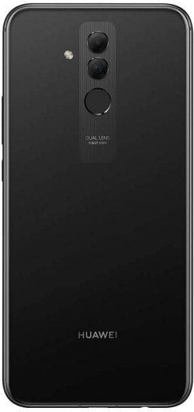
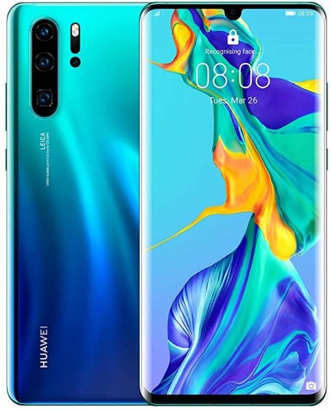
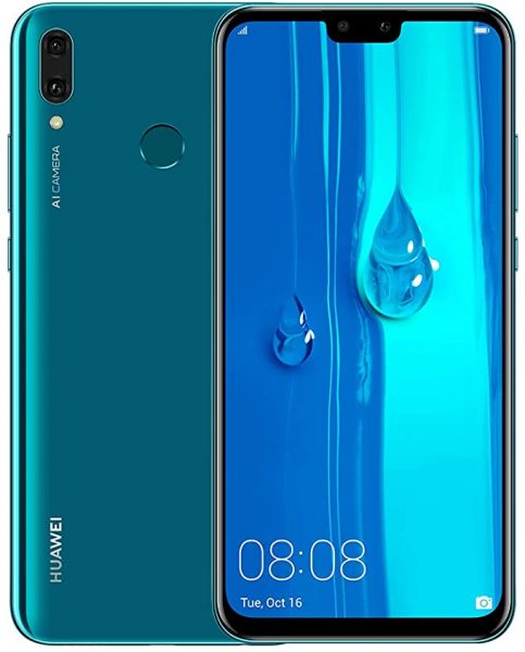
China’s homegrown brand Huawei is slowly becoming one of the biggest names in the industry. Though, Huawei is right behind Samsung with a market share of 19%. Its new releases receive glowing praise for good reason. Mainly because of their outstanding performing Huawei mobile phones in terms of design, camera specifications, and more.
OPPO
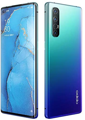
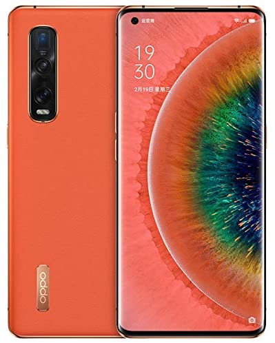
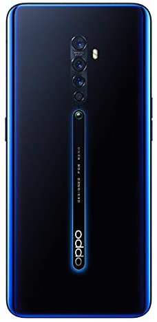
Oppo has been producing innovative phones since 2012. You might recognize the company for its “selfie phones.” Oppo created the first “Beautification” feature and rotating camera. Their mobile phone cameras have only increased in quality as time went on. Giving the brand well-deserved recognition as one of the best camera phones in the market.
Xiaomi
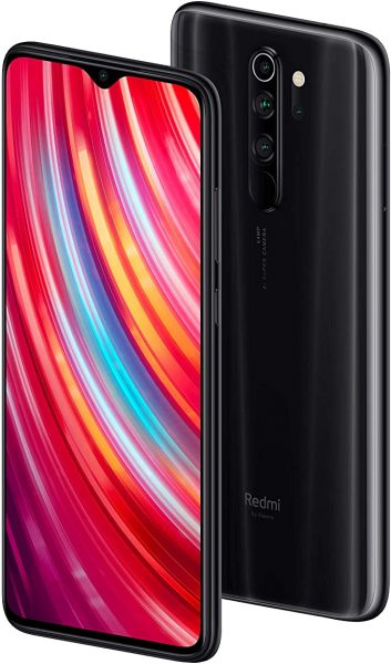
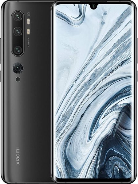
Xiaomi is slowly making its way around globally. As the prices for mobile phone spikes due to the demand, Xiaomi came in with only one goal — offering the best bang for your buck mobile phone. This brand features outstanding mobile specifications generally at a much lower price than many other mobile phone brands out there. Its flagship models include some of the best state-of-the-art cameras and fast processors. As a result, it gained a fair amount of popularity both locally and internationally. Xiaomi is now worldwide including Europe and the US. Find the best Xiaomi phones here.
Vivo
Yet another China-based phone brand that’s worth the shoutout. Vivo is known for its affordable yet innovative and high-quality phones. The company has been actively launching mobile devices that are targeting the mid-range market segment. Beyond its creative mobile phone designs, Vivo took-off mainly through its launches of selfie camera on a mobile phone. Most of their phones target beauty camera feature, triple cameras, in-display fingerprint sensor, and more. The upshot? Vivo phones come in vibrant colors and at much affordable prices. Though it gained its popularity worldwide, Vivo’s market focuses primarily on China and India.
Realme
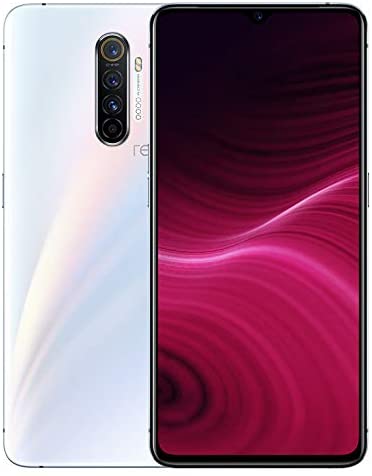
Although once under Oppo, Realme has recently made a name for itself in the industry. Realme rose to be the 3rd largest smartphone brand in India within 6 months of its release. Marketed towards “younger people of the world,” Realme produces affordable mobile phones. This doesn’t sacrifice its quality though. It’s modern phone designs and features fit right in the 21st century. Find the best Realme phones here.
Motorola
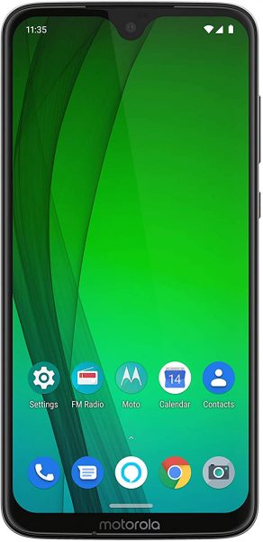
Most people would already know Motorola is the first in the world who introduces the commercial handheld mobile phone. From its conventional introduction mobile phone, Motorola has certainly come a long way over the decades. Beyond the chunky brick phones, Motorola has been actively evolving its technology to develop mobile phones that satisfy the demands.
Throughout the years, Motorola has proved its worthiness to be a great player in the mobile phone industry. Though it might seem that Motorola is falling behind, there are still plenty of recent Motorola’s mobile phones that are on par with Samsung, Huawei, and so on. As of now, Motorola market shares are strongest in India and Brazil.
Worth Mentioning Phone Brands
Just as if you thought that’s all the mobile phone brands, the truth is we’re not quite there yet. Here are some of the reliable brands that worth the mention. After all, you never want to be missed out on something that may pick your interest.
L.G.
LG is particularly famous for its large home appliances, but their mobile phones are as good as their other products. This mobile phone brand is especially famous for its flagship G series of smartphones in various functionalities that best suit the younger generations.
Nokia
Nokia has always been the largest mobile phone manufacturers but not until the introduction of iPhones and Android smartphones. Beyond its iconic Nokia 3310, Nokia now launches intuitive touchscreen display mobile phone with a resolution that is as good as many strong players in the industry. The upshot? Most of the smartphones are running on the latest Android OS, hence, you’re surely able to access any mobile apps as on other Android mobile phones.
HTC
HTC is a Taiwan-based manufacturer. It features an array of electronic devices that include laptops and eventually ventured into the mobile phone industry. Since its first commercial rollout of Android smartphones, HTC is now the primary manufacturer for both Android and Windows-based smartphones. The popular HTC collaboration is with Google through the introduction of Google Pixels. Alternatively, the HTC Wildfire series is worth the rave too.
OnePlus
OnePlus is drawing a massive crowd specifically with its dedicated quality of mobile phone and accessories. Their mobile phones were high-powered devices and proven to be durable. If you seek a mobile phone that can do justify the amount you’re paying for, OnePlus phones certainly won’t disappoint.
Lenovo
Lenovo’s primary business is the laptop and PC make. However, ever since the demand for smartphones rises, Lenovo took a turn to expand its focus on mobile phones as well. Despite its success, Lenovo also has a subsidiary brand for smartphones — Zuk in China. Some of the leading Lenovo mobile phones including the Lenovo Z6 Pro and Lenovo K10.
 Best OS For Your Mobile Phone: Android Phones vs iOS Phones vs Windows Phones
Users nowadays want something versatile and naturally, a mobile phone is bound to comply with the demand. That said, for a smartphone or mobile phone to function properly, it requires a backbone to support its function. While there is plenty of mobile operating system that can make it happen, the iOS, Android, and Windows OS is essential for a mobile phone function the way it should be. A worthy note is that not every OS is compatible with one another. That means, iOS is only made compatible with Apple’s phone and Android runs commonly on Samsung, Oppo, and more. But, which one is the best for you? Let’s examine it by category.
Mobile Phone Operating Systems
Operating Systems are the heart and soul of a mobile phone. The OS runs both software and hardware. Without it, phones would be futile. As of 2019, Android and iOS have dominated the OS market. Android takes up 74% market share and iOS takes up 25%, leaving about 1% for other mobile OS’.
For many loyal fans, the battle between Android vs. iOS vs. Windows is an age-old one. Moving from one OS to another is a big step, especially if you’re already in one ecosystem. If you’re interested to dive deeper into the analysis, here’s the ultimate breakdown of Android vs. iOS.
Mobile Phones with Best Apps
Apps are what make your smartphone your mobile phone. Your calls, texts, games all come from different apps downloaded on your phone. Each OS has its store you can get these apps from.
Here is the number of free apps in each store as of now, according to Statista:
| Mobile Phone Types | No. of Apps in Store |
|---|---|
|
2.5 million
|
|
|
1.8 million
|
|
|
669 K
|
|
Android is taking lead with over 2 million apps in the market. Famous for diversity, Android has a wide range of apps to choose from. You can check out our lists of productivity apps and video-editing apps to get you started. You can probably find anything you can think of, no matter how random it may seem. Its stock apps aren’t too shabby either. Some Android apps come built-in with Google’s default apps including Google Maps and Drive, to name a few.
Apple iOS running mobile phones have a decent competitive selection as well. Though Android has more apps, iOS apps tend to have better quality. Some developers create apps for iOS first, knowing that a majority of Americans use Apple. Apple’s iPhones and devices are also pretty much synced across the board. The OS updates the same for a majority of iPhone generations compared to Android phones. This means that there are apps available only for specific types of Android phones.
Windows comes in last with over 600,000 apps. You can find all of the standard apps like Spotify, Facebook, Twitter, Instagram. That means Windows phone user might encounter some problems searching for not so popular applications.
Apps Store
As aforementioned, iOS apps have better quality compared to Android or Windows. This is largely due to its intensive application process. Submitting an app for review on Apple’s App Store isn’t as easy as you think. The App Store’s filtering system is very selective.
Google’s Play Store is a bit more versatile. This may mean that not all apps are completely secure. Though Google has Play Protect to scan your phone for harmful apps and malware. The Play Store also has a refund policy, allowing you to rescind any purchases within two hours.
It’s also easier to use Play Store alternatives, should you not find the app you want there. Android phones support APK, though Android isn’t responsible for any viruses.
Like we said earlier, the Windows store is pretty basic compared to Android and iOS. It doesn’t have as inclusive of a catalog, making it hard to find niche apps.
The Mobile Phone’s Ease of Use
A mobile phone interface is highly dependent on the OS. By default, these OS are distinguishable and distinctive from one another. With iOS’ signature fonts and app design; Android’s customizable home page; and Windows’ iconic tile design.
Many mobile phones are running on Android, so the GUI varies from phone to phone. It also has a ton of customization options, such as widgets and skins. A downside to this would be the complicated toggles. If you want heavy customization and don’t mind messing around with settings, this is perfect.
Windows’ sleek design has a seamless integration to the Windows PC interface. If you use the Windows ecosystem, navigating through the mobile shouldn’t be a problem. Its simplistic GUI makes it perfect for any beginner. However, there’s a limit to customization.
While iOS has its moments, the Apple iPhone interface has stayed consistent throughout. There’s less of a learning curve when it comes to upgrading your iPhone. It also doesn’t have as many customization options as Android mainly for security purposes.
With Android cutting it close, iOS has a superior interface. Compared to Windows, iOS has better customization options. And it’s not as complicated to navigate through like Android.
Mobile Phones with best voice assistant
Contrary to popular belief, voice assistants have been around since the ‘60s. It wasn’t until Apple’s launch of Siri in 2011 that made it accessible to the public. Since then, many OS has come up with their voice assistant feature.
While Apple has Siri, Microsoft has Cortana that was introduced in 2013, named after an AI from Halo. As for Google, it launches Google Now in 2012 but eventually developed Google Assistant. Usually awakened by a voice prompt, these AI can act as a personal assistant. They can check the weather, look things up, and schedule appointments. Google is even developing an AI that can even converse with people. It’s a big step for technology, which is great but scary at the same time.
| Features | Google Assistant | Apple Siri | Windows Cortana |
|---|---|---|---|
|
Search Engine
|
Google
|
Safari
|
Bing
|
|
Voice Recognition Speed
|
Fast
|
Fast
|
Slower
|
|
Task Prompt
|
✘
|
✔
|
✘
|
|
Continuity / Follow-up Questions
|
✔
|
Yes
|
✔
|
|
Ecosystem Integration
|
Yes
|
✔
|
✔
|
Each Voice Assistant performed well with their tasks. However, Google Assistant and Siri surpassed Cortana by a mile. While all could answer queries, Cortana couldn’t detect voice in noisy environments.
Both Siri and Google Assistant could understand context and answer follow-up questions effectively. Apple’s Siri earns extra points for its automatic task prompt when asked a question. And all assistants have good ecosystem integration. Siri proved to be a more in-depth assistant than the other two. Its seamless transition from query to a task is great. Overall, a well-rounded assistant that works in any Apple gadget.
Bugs and Fixes
Android’s updates on a mobile phone are a bit slow and inconsistent. Because many phones run on Android OS, not all of them get quick updates. If you have a Vivo phone, your apps may not update as quickly as Huawei, for example.
As of 2020, Windows is cutting its updates on the Windows phone. Its final update was in January of this year. The update was for improvement and fixes. You can still use your Windows phone, but some apps might not work overtime.
Of all three, iOS updates are more frequent and consistent. Updates get synced to all iPhones. Up until recently, this included iPads. But Apple announced that iOS 13 would be exclusive to the iPhone this year. The iPad will get separate updates from the iPadOS.
Security and privacy
In today’s digital age, it’s harder to keep track of your security and privacy. Our smartphones store a ton of sensitive information. Which is why tech giants are working to ease our worries. In 2017, Nokia released a Threat Intelligence report. They found that a big percent of Android mobile phones suffered malware infection. This was closely followed by Windows. iOS only had about 3% of the findings.
There has been a lot of controversy surrounding Google and ads. There have been claims of Google selling user data to brands. Google removed about 600 adware apps in the Play Store with stricter app guidelines. Of the three, a mobile phone that is operating on iOS is the least prone to viruses and malware, making it the safest option.
Mobile Phone Peripherals
Peripherals can enhance the connectivity of your mobile phone. There are plenty of accessories you can get for your Android phones or iPhones but it’s all down to its incompatibilities of the phone models and brands.
Both Android and Apple have their smartwatches. Windows has yet to make its own. Some phones are now going wireless. There is a ton of support for Bluetooth earphones and headsets. Apple even recently received backlash for removing their 3.5mm headphone jacks. You may need to buy extra adapters, or get the new AirPods. Either way, it can be a bit more pricey compared to Windows and Android. In terms of connectivity, Android phones use standard USB cables. It’s much more universal than the iPhone’s lightning cable.
mobile Battery Life and Charging capabilities
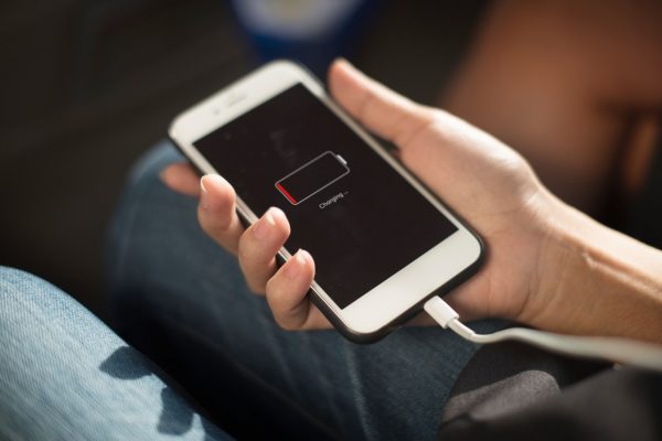
Both Android and iOS phones have comparably good battery life. But there is still a bulk of Android phones in the market that have better battery life. Windows phones have decent batteries, but they drain more easily. Charging time also takes a bit longer than with Android or iOS phones.
Recently, the latest iPhones support wireless charging and lightning charge. This was previously an area Android dominated in. However, Apple’s lightning cable might not be as durable. Hence, that would be an add-on cost to replace your mobile phone cable. Whereas this is already included with Android phones.
Mobile Phone Storage capacity
If you’re someone who has a lot of videos or saved memes, you need bigger phone storage. Fortunately, today’s smartphones are capable of hundreds of GB of storage. 128GB phones are becoming industry standard as of late. Samsung has already developed 1TB phone storage. The future of bigger storage capacity is bright.
While both Windows and Android allow storage expansion, the iPhone does not. Apple wants to keep the iPhone’s design sleek and minimal. This makes it hard to remove the iPhone’s battery or add an external SD card.
In terms of storage capacity, Android definitely takes this win. It wins us over with great support for storage expansion. Not to mention bigger internal storage on the horizon.
Video Conferencing
Video conferencing is an easy way to coordinate with digital teams. Or, just talking with family and friends overseas. All three OS have their apps for video conferencing. Apple’s iOS has FaceTime, Android has Google Duo and Windows has Skype.
iPhones have FaceTime built-in to the phone. It’s also built-in to all Apple devices like the iPad and Mac. You can answer a Facetime call both in any of your Apple devices. It will alert all of them if there is a WiFi or data connection.
Most Android phones with Google Suite have Google Duo built-in. It’s Google’s latest video conferencing app, replacing Google Hangouts. The app is cross-platform and can also be used with iOS. Google Duo’s “Knock Knock” feature is unique. It allows the person you’re calling to see you before they answer.
You might have to download Skype on your Windows phone. But it has more functionality than Facetime and Google Duo combined. Skype’s group call can include up to 25 people and allows instant messaging during the call. It also has a ton of features like screen share, voice messages, and more. There’s a reason Skype is widely used and trusted by many.
Camera Software
It’s hard to say whether Android cameras are inherently good or bad. There are a ton of great cameras, but a lot of bad ones, too. There are a lot of customization options for Android though. And there are lots of apps to maximize camera settings as well. Plus, Google Photos have unlimited storage, so it’s easier to manage.
The iPhone consistently gets praise for its great camera quality. They take sharp and well-saturated photos. The recent releases have cleaner Portrait Mode, wider angle than most Android cameras. There are also a lot of great editing apps on the App Store to improvise any pictures.
Windows phones surprisingly have good quality cameras. It may not take pictures as crisp as the iPhone, but they have many cool features. Their wide-angle lenses are great for taking pictures with friends.
The overall winner for best mobile phone type
It was a close call, but iOS wins this showdown in terms of these criteria. But we admit that it’s hard to be completely objective. If you’re looking for something simple and secure with a great ecosystem, then choose iOS. If you want something more customizable with better storage, pick Android. And lastly, if you want something more minimalist and easy to navigate, then pick Windows.
Types of Mobile Phones
Many of us would have though a mobile phone or a smartphone is a wonder in a pocket that does everything we command. While it true that most smartphone does the basic job but some are designed specifically to outshine the rest. There are plenty of different mobile phone types but here are some of the ones that we narrowed down.
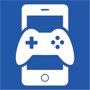
Gaming Phones
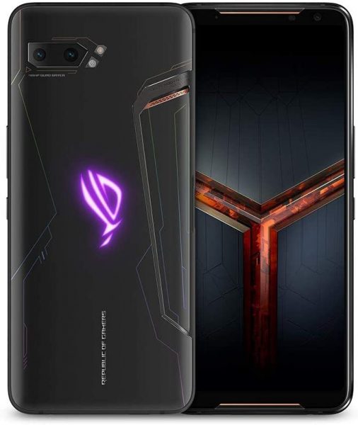
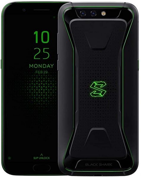
As its name suggests, a gaming phone is made to cater to your gaming needs. These gamers-oriented phones emphasize on mobile phone specifications, displays, processors, and its design. Generally, gaming is the most processor-intensive activity you can possibly do on a mobile phone. So by default, it makes sense that gamers alike would like to spend a little more on an ideal mobile phone with enhanced performance. Find out which are the best gaming phones to invest in now.
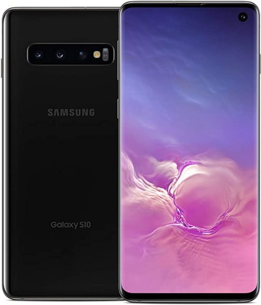
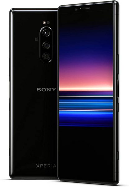
Camera Phones
With the rise of social media, it’s hard to find anyone with a mobile phone not to be uploading any photos or videos nowadays. That said, it’s also unavoidable that some of your jobs might require you to utilize your camera features. While it is true that almost every smartphone, cell phones, and mobile phones come with a camera. But, not every one of them is the best. If you’re considering a camera phone, the camera specifications on a mobile phone is highly dependent on the mobile phone brands, quality of the lenses, it’s software too.
However, due to the increasing demand for a camera phone, there are plenty of options available in the market now. Beyond the leading brands like — Huawei, Apple, Samsung, newcomers like Vivo as such is a great option too. Depending on your budget and the purpose of a camera phone, whether it’s for professional mobile photography or selfies, there’s always something for you. Ultimately, you get what you paid for. So, remember to do your homework before making your decision.
Heavy Duty Mobile Phone
Just to clarify, we’re not referring to the ancient heavy-brick phone here when we’re discussing a heavy-duty phone. In fact, in our opinion, a heavy-duty phone should be able to sustain your intense mobile activities and the way of handling a mobile phone. A long battery life mobile phone is a great example in this case. What it does it to provide a larger battery capacity to support your entertainment activities like gaming, video streaming, video calling, and more.
While most mobile phones claim that it has a long battery lifespan but there are some which are made specifically with extra battery capacity to accommodate your needs. A great example includes the Huawei P30 Pro and iPhone Pro Max. Not only it has an impressive battery lifespan, but it’s also waterproof to give you the security even during the harsh weather. Find out which are the best waterproof phones here.
Music Mobile Phones
Every mobile phone plays some sort of music or ringtones. But let’s admit that not all of them are the best nor impressive. We find most of the mobile phone manufacturers cut corners in audio specs to save some costs. Indeed, a good sound system is not cheap and that applies to a mobile phone too.
So, to look for a good music mobile phone, a good measure is to get familiar with some of the specs and to test out the stereo in a store. Apart from that, here are a few specifications you should be looking out for in a music mobile phone.
- Audio enhancement
- Audiophile sound customization
- Internal speakers
- Speakers design
- Wired audio quality
 Mobile Phone Tests To Help You Make Better Buying Decision
The last thing you want is a mobile phone that doesn’t last. Of course, you want your money worth by getting what you paid for. But the question you should be asking is if your mobile phone delivers what it claims?
Here are some of the best mobile phone tests to help you make the best choice. While some we did it on behalf and some of them you can perform it yourself on your mobile phone.
Software Tests
It’s essential to test the performance of the mobile phone and the best way to do it is by running a software test. All of these tests are pretty straight forward and it should tell you exactly where went wrong. Regardless if it’s about the uncertainties of the mobile reception, processor performance or skepticism of the mobile displays. Run these tests and it shall give you the answers you need to make sure you get what you paid for.
Reception Test
The most basic function of a mobile phone is calls and texts. With a bad signal, it’s hard to do either. Bad signal affects even internet connectivity. To test or establish a baseline for the reception, you can do the following test:
Sound Quality Test
It’s also important to have great sound quality on any phone whether it’s for a phone call or music listening purposes. Topnotch design and features are useless if you can’t listen to a thing. To test the sound quality, you can check out this video:
Mobile Display Test
This video will help you check out the display quality of your screen. All you need is to go to your phone, click this link and play the video. This is in 4K for optimized viewing.
Mobile Phone Battery Life Span Test
Having a long-lasting battery can take you a long way. Literally. You can take a phone with a durable battery on long road trips without breaking stride. This is also useful for long mobile gaming sessions. Check out this battery life test on top phone brands:
Connectivity Test [WiFi & Bluetooth]
In this generation, Wi-Fi is our lifeline. Data can drain too much battery and cost a lot, so we sometimes tend to rely on Wi-Fi. A simple connection test can prove whether your phone is capable of connectivity. You can try to download something to see how fast it gets. The best way to test your WiFi connectivity to your phone is by using a network speed test app. As for Bluetooth connectivity, try to pair with multiples Bluetooth devices including your Bluetooth headset, speakers, and so on. To test the Bluetooth strength, you can step away from one distance to another to find out how reliable it is.
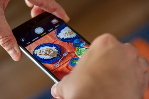
Camera Quality Test
Smartphones make mobile photography easier. You can take and edit pictures anywhere and anytime. While to begin with, you first need a good camera on your mobile and the indication of a good camera quality has to produce sharp and clear images. Besides, it should also have great color saturation. You might also want to consider the aperture, shutter speed, the camera ISO, zoom capabilities, and so on. The best way to test out the camera quality is by taking multiple photos in the same settings including the angle and lighting, trust your eye to see if the results are consistent.

Hardware Tests
A good way to test mobile phone durability is the outer shell of a phone. Besides its software, the next question you should be asking if the exterior is reliable enough to sustain those rough handling? As for the worst, will it break under certain circumstances? These are factors you may want to consider when choosing your ideal mobile phones.
Drop Test
Most phones boast on their high durability. But there’s only one way to find out their claims are true. Of course, you don’t want to do it yourself and consider yourself lucky because there are plenty of phone drop tests where you can compare your desire mobile phone models side by side. What you want to prove from this test is whether the phone can withstand casualties like phone slipping out of your pocket and fell from a great height. Also, to what extent the mobile phone still survive after suffering from the damages.
If you consider yourself an active person or somewhat careless occasionally, the drop test is crucial to help you make a better buying decision.
Scratch Test
We know how annoying it can be when your brand new mobile phone gets scratched. Whether it’s a scratch on the outer sheet or the screen, a scratch is a scratch and it’s not recoverable unless you replaced it with brand new spare parts. So, to make sure your money is well-spent, you might want to opt for a mobile phone that offers scratch-proof features.
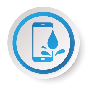
Water Resistant Test
There’s a fair amount of mobile phones nowadays that offer water-resistant features. But, how reliable it is? The only way to find out is by testing it out. Again, if you don’t want to test it on your mobile phone, you can also opt to watch some comparative videos to test out the resistance of the mobile phone against water splashes and as to how deep a waterproof mobile phone can submerge in the water.
 Top Android Phones That’ll Make Your Money Worth
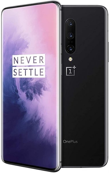
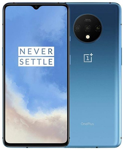
OnePlus 7 Pro – Best for Gaming
With its wide 6.67” screen, the OnePlus 7 Pro is perfect for gaming. It comes without bezels or notches that can distract you while in-game. Besides, it is with a concealed camera that you can draw up when needed. On top of that, it also has up to 12GB RAM with 256GB of storage and a 90Hz refresh rate. OnePlus teamed up with eSports players for this, so it’s optimized for mobile gaming.
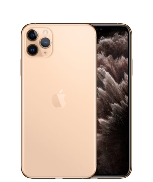
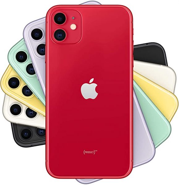
iPhone 11 Pro Max – Ideal for Photography
Camera phones have made it easier to do photography nowadays. If you’re looking for a high-quality phone camera with excellent specs, the iPhone 11 Pro Max is for you. Its smooth-running camera gives you high-resolution pictures both day and night. Its rear camera has a 12 MP “wide” camera with f/1.8 aperture with optical image stabilization (OIS) 12 MP “2x telephoto” camera f/2.0 aperture with OIS. Another add on is it also offers 12 MP “ultra-wide” camera with f/2.4 aperture and 120-degree field of view. The photo quality is crisp and well saturated even without editing.
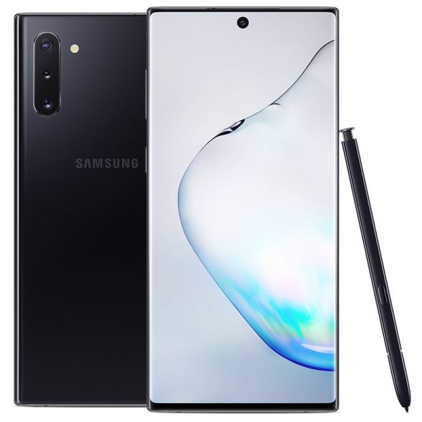
Samsung Galaxy Note 10 – Great for Entertainment
If you’re a cinephile and a loyal streamer, the Samsung Galaxy Note 10 is for you. Its impressive 6.8-inch screen will surely leave an impact. It also supports Netflix’s picture in picture features. This allows you to multitask while watching your favorite shows. The fill-to-zoom works especially well with this widescreen. Note 10 supports HDR streaming from Netflix, Hulu, Amazon Prime, and YouTube as well. YouTube also takes advantage of the 1440 resolution and can give you up to 60 fps of streaming.
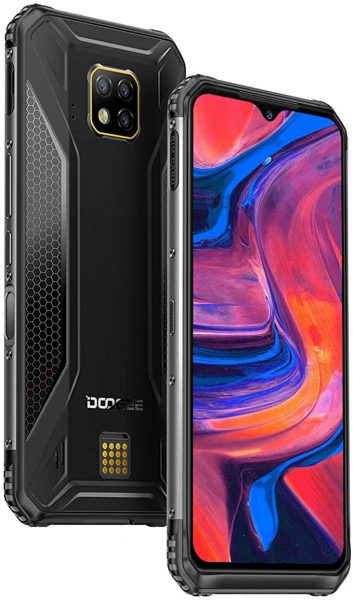
Doogee S95 – Best Suit your Active Lifestyle
The Doogee S95 Pro can keep up with any active lifestyle. It comes with many features more than any rugged phone. To top it all off, it has a very durable casing that can survive any drop. The S95 Pro’s waterproof, dustproof, and heatproof quality is military-grade. And the phone isn’t as hefty or bulky as you would expect.
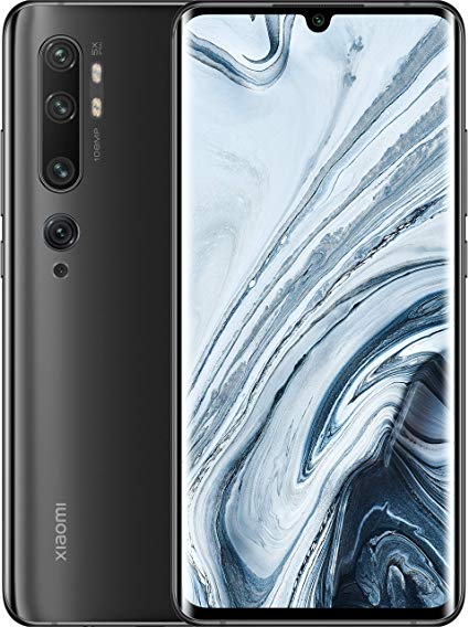
Xiaomi Note 10 – Outstanding Long Battery Lifespan
Hate constantly charging your phone? You should check out Xiaomi Mi Note 10. This affordable phone has a long battery life with over 5260 mAh that you can use for two days. It supports fast charging in just under 65 minutes.
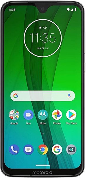
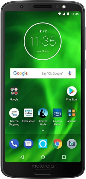
Motorola Moto G7 Power – Budget and Wallet-Friendly
If you want a phone that won’t compromise quality for its price, the Moto G7 Power is for you. It may not have the best camera, but it’s great for its price. It also has a colorful display that is perfect for viewing. At its price range, the Moto G7 has many features other mid-range phones don’t offer.
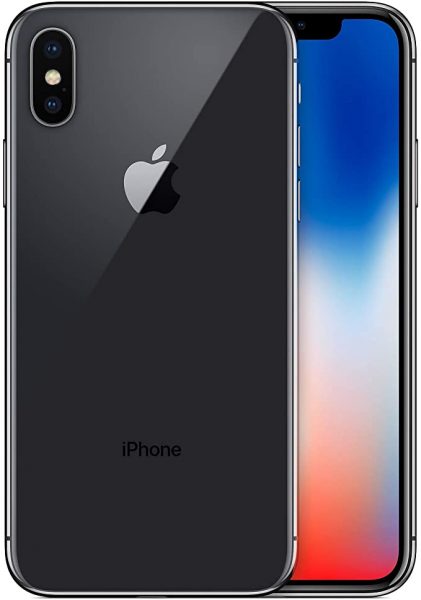
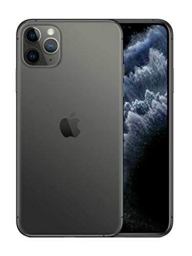
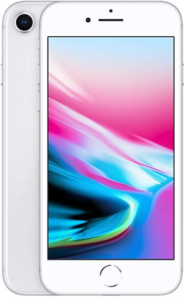
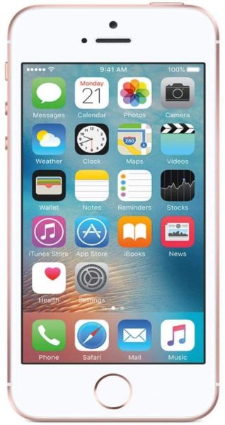
Best iPhones [Pros & Cons Analysis]
| Models | Pros | Cons | Next Step |
|---|---|---|---|
|
|
||
|
|
||
|
|
||
|
|
||
|
|
||
|
|
||
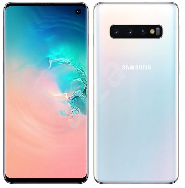
Top Samsung Phones [Pros & Cons Analysis]
| Models | Pros | Cons | Next Step |
|---|---|---|---|
|
|
||
|
|
||
|
|
||
|
|
||
|
|
||
Conclusion
Choosing the right mobile phone isn’t as simple as you may think. There is a lot to think about, both in hardware and software. We’ve listed our top picks based on many factors. But at the end of the day, it’s your phone. We hope these tips and tricks help you find a phone that best fits your lifestyle and preferences.
Mobile Phone FAQs
Android is one of the most popular mobile phone OS’. Android named their OS versions after desserts, with the latest being Oreo and Pie. It was first created in 2003 by Android Inc. and was eventually acquired by Google.
The Google Pixel 3 XL and iPhone 11 Pro Max has excellent camera quality and runs on Android OS. You can check out our list of best camera phones here.
Steve Jobs first introduced the original iPhone on January 9. 2007. The model itself hit the shelves on June 29 of the same year.
With every release of mobile phones come promises of less lag. We like to think we’ve come pretty far in terms of addressing lag, but it’s still inevitable. Phones and their components grow old, slowing down phone performance. Another reason is that there might be apps running in the background eating up RAM. You can check app permissions to toggle which apps can run in the background. You might also have full storage or failing phone memory.
If you have many apps on your phone, this contributes a lot to the battery drain. Leaving apps running in the background can drain your phone. Having your brightness on full power can also lead to the battery drain. Constant notifications lighting up and making sounds are also a big factor. Double-check your app settings for optimal battery usage.
You can check out some battery-saving apps to help you manage your battery use.